



The AI compute supply chain is bifurcating into two parallel systems. One runs on private capital, market-based financing, and a Dutch lithography monopoly. The other runs on state capital, strategic allocation, and an indigenous substitution program built under export controls. Both converge at a single company whose machines neither stack can yet build for itself.
This is what the dependency map shows when you trace every edge from capital to silicon to model. A hundred and two companies. Five thousand relationships. Every one sourced.
Update, Aug 26: hours after this piece published, a stealth model that had spent a week atop OpenRouter’s usage leaderboard was confirmed as Zhipu’s GLM-5.3-Flash, and the company said every token of that traffic was served on Chinese chips. The China-models layer, the Huawei count, and the Jalapeño benchmarking below are updated to match the graph; the event is this piece’s software-separation finding made live.
The short version
The West builds AI compute on private capital; China builds it on state allocation. Both stacks bottleneck through ASML, and beneath ASML through two private German firms. You can escape TSMC. You cannot escape ASML.
The chain narrows as it deepens: many labs and clouds at the top, one laser supplier and one mirror supplier at the base, permitted power constraining everything above.
China’s software gap is closing faster than its hardware gap, because iteration beats capital expenditure. Faster is still years, not quarters, and the hardware gap remains the multi-decade problem.
NVIDIA is simultaneously the strongest and most fragile node in the Western stack: every large customer depends on its toolchain while building alternatives to its chips, and its financing platform bets on demand never softening.
The freshest evidence cuts against indigenization: Xiaomi’s flagship XRING chips, framed as a self-sufficiency breakthrough, are all fabricated by TSMC. The newest cross-stack edge deepened instead of thinning.
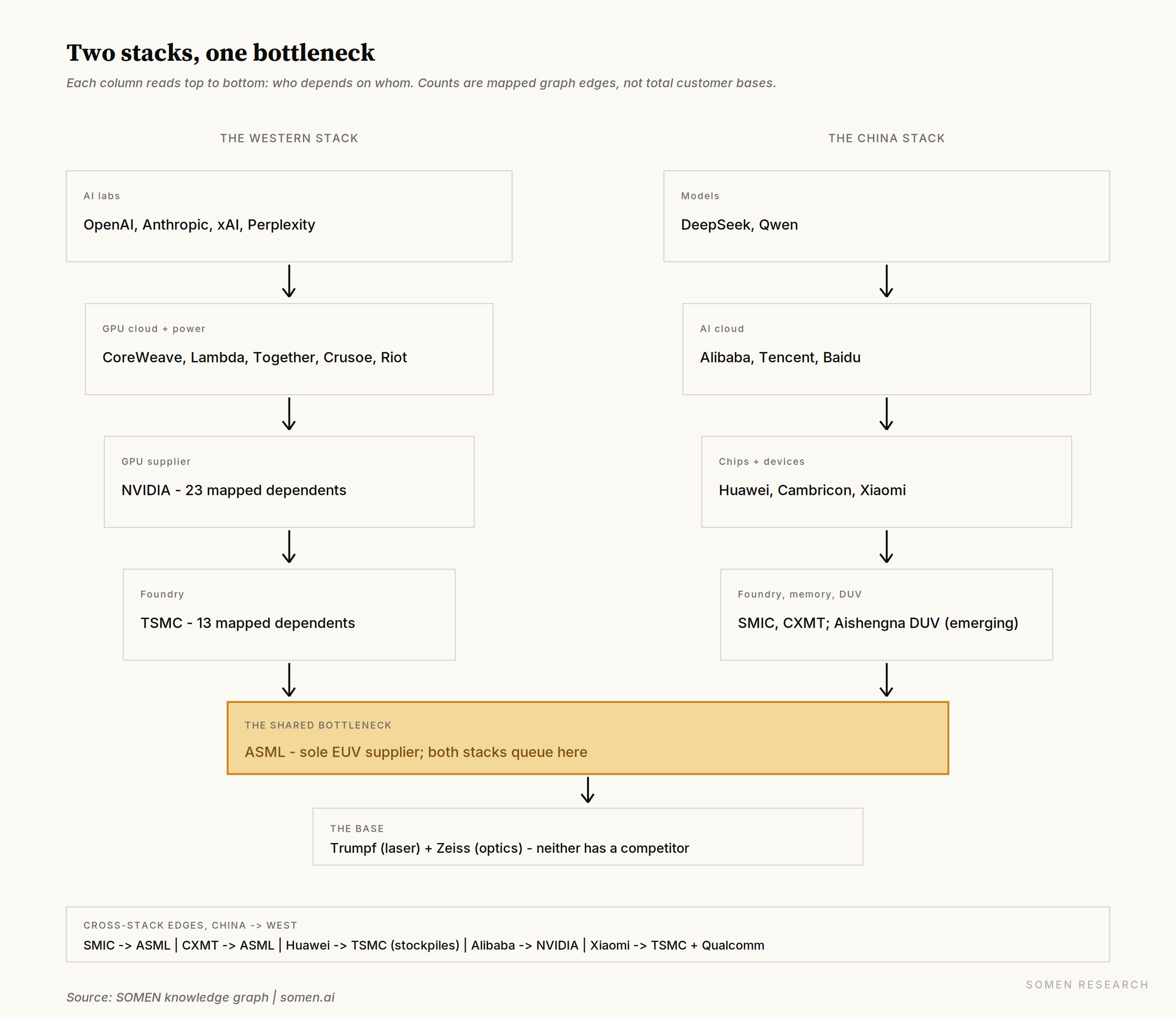
The Western Stack
The Western AI compute supply chain runs through six layers, each dominated by one or two companies that the next layer cannot operate without.
Layer 1: The deepest bottleneck. Trumpf makes the high-power CO2 lasers that drive ASML’s EUV light source. Carl Zeiss SMT makes the mirrors that focus it. Both are private German companies. Neither has a competitor. The EUV scanner is widely considered the most complex machine ever built. It fires a high-power laser at 50,000 microscopic droplets of molten tin per second, creating a plasma that emits 13.5nm wavelength light, collected by the smoothest mirrors ever manufactured (atomically smooth, sub-0.1nm roughness), all in a vacuum. Each scanner costs $200 to $300 million and weighs 180 metric tons. ASML spent 20 years and billions of euros developing EUV. Its foundational EUV patents, filed during the 1990s consortium era, have already expired; the moat held anyway, because no single patent covers the machine, the tuning algorithms stay trade secret, and the active estate (more than 38,000 patents, refreshed at roughly 2,000 filings a year) runs on continuous filing rather than any one expiration date. Without Trumpf’s lasers and Zeiss’s optics, ASML cannot produce EUV scanners. Without EUV scanners, TSMC cannot produce advanced chips. The dependency chain starts in two family-owned companies in Ditzingen and Oberkochen.
Layer 2: The sole EUV supplier. ASML is the only company on Earth that manufactures EUV lithography scanners. It recognized revenue on 48 EUV systems in 2025, out of 327 lithography systems in total. Delivery of a single EUV scanner requires 3 Boeing 747 cargo flights. The next generation, High-NA EUV, is already shipping to Intel for the 14A (1.4nm) process that Terafab plans to license. There is no alternative to EUV. Canon’s nanoimprint lithography works for memory, not for logic chips. Electron-beam lithography is too slow for volume manufacturing, at hours per wafer versus EUV’s 150-plus wafers per hour. The semiconductor industry’s own roadmap (IRDS) assumes EUV remains the patterning technology through at least 2036. No replacement exists on any credible timeline.
Layer 3: The dominant foundry. TSMC fabricates the chips for every major Western AI company. The twelve became thirteen in June, when OpenAI unveiled Jalapeño, its first in-house inference chip, fabricated on TSMC N3 with CoWoS packaging. The thirteen in this graph that depend on TSMC: NVIDIA (100% of GPUs on N3 and N4P), Cerebras (wafer-scale), Groq, SambaNova, Etched, OpenAI, Xiaomi (all three XRING chips), Huawei (legacy Ascend dies stockpiled before sanctions), and Terafab (current Tesla AI5 fabrication, the very dependency its Texas fab is built to replace), plus capacity competitors Apple, AMD, Qualcomm, and Broadcom. Samsung Foundry and Intel Foundry are alternatives, but TSMC holds approximately 90% of advanced-node market share. Samsung has lost major customers (Qualcomm moved Snapdragon back to TSMC). Intel Foundry counts announced external customers, Microsoft among them on the 18A node, but has yet to record meaningful external revenue. Terafab would be the first at scale.
Layer 4: The sole high-end GPU supplier. NVIDIA designs the chips that power every frontier AI training run. All NVIDIA GPUs are fabricated at TSMC. Twenty-three companies in this graph carry direct NVIDIA dependencies: the GPU clouds (CoreWeave, Lambda, Together, Crusoe), frontier labs and model builders including SSI, Thinking Machines, Skild, Atoms, Starcloud, OpenAI, Perplexity, Mistral, and Cursor, Alibaba’s AI cloud, Scale AI, Blue Origin, Valar Atomics, and Riot, plus the five hyperscalers themselves, Microsoft, Amazon, Google, Meta, and Oracle, whose procurement the graph now records as direct customer edges. Four of those hyperscalers are also building custom silicon: Microsoft has Maia 200 (in Azure production, serving OpenAI models), Amazon has Trainium3 (shipping), Google has TPU v7 (deployed at scale for inference), Meta has MTIA (four generations in deployment). None has displaced NVIDIA for frontier training. The newest escape attempt is the purest: OpenAI’s Jalapeño inference chip, announced in June and benchmarked in August at 1.5 to 1.9x more AI work per watt than NVIDIA’s GB300 racks for serving, was designed with Broadcom and runs on TSMC N3 with CoWoS packaging. It escapes NVIDIA for inference and lands directly on the layers beneath. SemiAnalysis, invited into the labs, found more beneath: a revised stepping already in the fab at roughly 25 percent better performance per watt, and single-token throughput per megawatt beating Vera Rubin’s published figures. The dependency map shows why: custom silicon still requires TSMC fabrication, which still requires ASML lithography. The customers are trying to escape NVIDIA, but they cannot escape the supply chain NVIDIA sits inside.
Layer 5: The GPU cloud layer. CoreWeave, Lambda, Together, Crusoe, and Riot Platforms deploy NVIDIA GPUs for AI training and inference. All depend on NVIDIA hardware, which depends on TSMC fabrication, which depends on ASML lithography. Anthropic signed a 20-year, $9.1 billion lease for 191 megawatts at Riot’s Rockdale, Texas campus. The bitcoin miner is now an AI infrastructure landlord, converting a 1.7-gigawatt Texas power portfolio from cryptocurrency to compute. Crusoe is building 2.1 gigawatts of AI data-center capacity in Abilene for the OpenAI Stargate initiative and a separate 900-megawatt campus for Microsoft. Valar Atomics is developing nuclear SMRs that directly power NVIDIA Blackwell chips, with a 30-megawatt waterless AI factory in Utah.
Power is the binding constraint on all of this. Goldman Sachs projects data-center electricity demand growing at 15% annually, reaching 8% of total US electricity consumption by 2030. Every gigawatt of AI compute requires permits, grid connections, cooling infrastructure, and years of construction. The companies that control permitted power (Riot: 1.7 GW, Crusoe: a reported 7 GW pipeline, Talen Energy, Constellation) hold an asset that AI labs cannot manufacture or code their way around.
Layer 6: The AI labs. OpenAI depends on Microsoft Azure for compute. Anthropic depends on Amazon AWS and Google Cloud. xAI merged into SpaceX at $250 billion and runs its Colossus training cluster on Oracle Cloud. Perplexitycommitted $750 million over three years to Microsoft Azure for frontier model access.
Anthropic’s compute procurement in three months reportedly totaled over $60 billion in contracted commitments, and the instruments differ: a reported $45 billion compute arrangement with xAI, a lab buying inference from another lab; $10 billion in capacity commitments with Volta Infra; and the one filing-verified leg, the $9.1 billion 20-year lease at Riot. The composite is directionally useful; only the Riot leg is documented in a public filing. The labs sit at the top of a dependency chain that runs through clouds, through NVIDIA, through TSMC, through ASML, through Trumpf and Zeiss.
The China Stack
China is building a parallel supply chain at every layer. The ambition is documented: Xi Jinping’s April 2025 Politburo session called for “self-reliance and self-strengthening” with an “independent and controllable ecosystem across hardware and software.” Huawei founder Ren Zhengfei’s stated target: 70% self-sufficiency by 2028.
Layer 1: Lithography. SMEE, China’s oldest lithography maker, ships 90nm-class dry ArF scanners. Aishengna, a state-owned venture that absorbed SMEE’s and Huawei-linked Yuliangsheng’s engineering teams, has begun mass production of immersion DUV scanners, targeting roughly five units in 2026, with 20 planned for 2027; the first units go to SMIC, Hua Hong, and CXMT for production-line validation rather than volume output. The machines still use imported Japanese components. A Shenzhen lab has an EUV prototype that generates photons but has not exposed a wafer. More than 3,000 researchers reportedly work across the program. Beijing’s target for chip output from the domestic EUV machine is 2028; Reuters’ sources call 2030 more realistic.
ASML recognized revenue on 327 lithography systems in 2025, 48 of them EUV. China’s entire domestic lithography program produced five immersion DUV tools.
Layer 2: Foundry. SMIC produces 7nm chips using DUV multi-patterning, a technique that achieves smaller features through repeated exposures on older equipment. The cost is punishing: approximately 40 to 50 percent more expensive than TSMC’s equivalent process. External estimates (SMIC publishes no yield data, and no two analysts agree closely) put the mature 7nm line near 50 percent yield, falling to 20 to 40 percent on the 5nm-class node where multi-patterning compounds. Treat the percentages as informed inference, not measurement. Huawei is building three of its own fabs in Shenzhen’s Guanlan district, but the first was not expected at full operation before 2026, relying heavily on untested domestic equipment. SMIC co-founder Wang Yangyuan and the heads of YMTC, NAURA, and EDA firm Empyrean jointly described China’s tool industry as “small, fragmented, and weak” in March 2026 and called for national consolidation. Big Fund III’s $47.5 billion is reportedly being redirected toward lithography and EDA as a direct response.
Layer 3: Chips. Huawei is China’s leading AI chip designer. Huawei markets the Ascend 910C as H100-class; a single third-party test by DeepSeek measured it at roughly 60 percent of an H100 for inference, with sustained training reliability the weaker suit. Huawei’s compensation is scale: system-level clusters like the 8,192-chip Atlas 950 SuperPoDtrade silicon efficiency for interconnect and aggregate throughput. The Ascend 950PR targets 2.8x the H20. Huawei plans 600,000 Ascend chips in 2026 and expects $12 billion in AI chip revenue. Cambricon is second, planning 500,000 Siyuan accelerators. China’s domestic chips made up a reported 41% of the Chinese AI chip market in 2025, up from under 10% pre-2023. NVIDIA’s share of China’s advanced AI accelerator market has collapsed. Eight companies in this graph depend on Huawei commercially, including DeepSeek, whose V4 model was the first frontier-class AI validated on Ascend hardware, and Zhipu, whose GLM-5.3-Flash just spent a week as the most-used model on OpenRouter, served entirely on domestic silicon.
Layer 4: Software. Huawei’s CANN (Compute Architecture for Neural Networks) is China’s CUDA alternative. Open-sourced in December 2025, it claims 4 million community members by Huawei’s own count (a metric spanning registered users of the broader Ascend ecosystem, not kernel engineers) and supports 70-plus models on release. The developer experience has moved from what one startup founder called “essentially a section of desert” to what he now calls a “youth phase.” AIGCode, a Shanghai AI coding startup, tried training a 7B-parameter mixture-of-experts model on Ascend in early 2025, hit a bug, and waited four months for Huawei support. By 2026, the same company achieved 65% Model Flops Utilization on Ascend during pre-training, nearly double the industry average. A major Chinese bank contributed 34 optimizations to vLLM-Ascend, the inference engine project, trusting Huawei chips with core risk-management processes. CANN Next adds a SIMT programming model that adapts directly to CUDA code, lowering the migration barrier.
DeepSeek V4 achieved 68 percent of H100 throughput on Ascend at 55 percent power consumption in reported inference tests (pre-training remained on NVIDIA-class clusters). The learning loop has started: each model adaptation makes the next one easier. CUDA took 15 years to build that loop. China is compressing it under export-control pressure.
Layer 5: Cloud. Alibaba holds a reported 35.8% of China’s AI cloud market. Tencent reportedly spent CNY 18 billion on AI in 2025 and planned to double it in 2026. Huawei has reportedly deployed over 300 Atlas 900 A3 SuperPoD systems (384 Ascend chips each) for 20-plus enterprise and government customers. Alibaba ordered hundreds of thousands of Ascend chips for DeepSeek V4 deployment. Tencent and ByteDance followed. The scale of domestic Chinese AI compute is larger than most Western analysts assume. The constraint is not demand or capital but chip supply: Huawei cannot produce Ascends fast enough to meet orders.
Layer 6: Models. DeepSeek is China’s leading open-source AI lab. V4 runs a 1.6-trillion-parameter mixture-of-experts architecture, activating 37 billion parameters per inference. The lab declined NVIDIA’s offer of early kernel access and chose to co-design its inference deployment with Huawei instead; V4’s pre-training itself still ran on NVIDIA-class clusters, a split that is itself the two-stacks condition in miniature. DeepSeek delayed the V4 release by three months to re-engineer inference for CANN. Its $7.4 billion first external funding round, at a $55 billion valuation, was funded entirely by domestic strategic capital.
The distinction did not survive the week. A free stealth model listed as Ox Alpha spent six days as the most-used model on OpenRouter, more than doubling DeepSeek’s traffic, until Zhipu confirmed it as GLM-5.3-Flash and open-sourced the weights: 320 billion parameters, MIT license, a newly trained multimodal base, at a tenth of its own flagship’s price. It was the fifth anonymous “Alpha” release in six months; all five resolved to Chinese labs. The confirmation carried the load-bearing fact for this map, in Z.ai’s own words: “all of this traffic was served on Chinese AI chips,” on a production disaggregated serving architecture across tens of thousands of domestically developed accelerators, with a claimed 3x end-to-end inference advantage over NVIDIA that is the vendor’s own number and unverified. It does not need to be verified to make the point. DeepSeek proved a frontier model could run on Ascend in a validated test. Zhipu proved the open market’s most popular model could run on domestic silicon at production scale, for a week, at free pricing. Zhipu is also the stack’s first listed lab (Hong Kong, January 2026; a market cap that touched the equivalent of $128 billion in June) and has sat on the US Entity List since January 2025.
The Edge
On August 24, 2026, Xiaomi added a seventh layer to the China stack from an unexpected direction: the consumer device. At its XRING chip conference in Beijing, the company showed the AI Cube Prototype, a 150-watt mini-PC that runs 120-billion-parameter and 3-billion-parameter models locally on three chips Xiaomi designed itself. The XRING O3 is a 3nm flagship SoC already in mass production for September’s Xiaomi 18 Fold, with a shipment target of 200,000 to 300,000 units. The XRING O100 stacks two DRAM wafers face-to-face on a 6nm logic wafer, hybrid-bonded at a 1.4 micron pitch, reaching 1.22 TB/s of near-memory bandwidth. The XRING D100 is a 3nm smart-driving chip that Xiaomi calls China’s first at that node, validated, with commercial use scheduled for 2027.
The program behind it is serious: more than 20 billion yuan ($3 billion) invested to date, a semiconductor design unit grown past 3,000 people, and a stated plan of at least $7 billion over a decade. Xiaomi joins Apple, Samsung, Google, and Huawei in the small club of device makers that design their own flagship silicon, and it is extending the same chip architecture into cars and robots.
Here is the part the dependency map records and the launch coverage mostly does not. Every chip in the lineup is contracted to TSMC per Reuters’ sources (Xiaomi itself confirms only the O3’s node, and left the D100’s foundry undisclosed at the unveil). The O3 runs on N3P, the same 3nm node as Apple’s current parts. The designs are Chinese. The manufacturing is not. Xiaomi has not reduced its exposure to the Western stack; it has converted a dependence on Qualcomm merchant silicon, which any foundry could fabricate, into a dependence on TSMC leading-edge capacity, which sits under American export jurisdiction and competes for allocation with Apple and NVIDIA.
The export-control fine print makes the arrangement more interesting still. US export rules presume denial when TSMC fabricates 7nm-and-below chips for Chinese designers, and shipments in that class are presumed to be AI chips unless proven otherwise. The XRING O1 cleared the presumption in 2025 through mechanical carve-outs: the die was packaged outside China and stayed under the 35-billion-transistor threshold. The D100 is an explicitly AI chip at 3nm for a Chinese automotive program. How it clears the presumption is unreported. The AI Cube is being read as proof that China can design chips as good as almost anyone’s. It is equally evidence that the fabrication gap this map shows has not moved: China’s newest design win converges on the same Taiwanese fabs as every Western AI company.
There is a Western counterpart to the Cube, and the comparison is exact. NVIDIA’s DGX Spark and AMD’s Ryzen AI Max systems run 200-billion-parameter models locally on 128GB of unified memory. Apple answered a day later. The Mac Studio M5 Ultra, announced August 25, runs models with hundreds of billions of parameters in up to 512GB of unified memory at 1.2 TB/s, a tier above the Cube’s 120-billion-parameter class, built on the same TSMC 3nm node family. The head-to-head the headlines invite is a trap: the Cube’s much-quoted 1.22 TB/s is the accelerator’s small near-memory pool, not the system memory its large model runs in, and that pool’s bandwidth was never published. The honest comparison cannot be made yet. Xiaomi’s route is its own three-chip stack running its own MiMo models. Same product category, similar parameter counts. The edge layer is the one place where both stacks already ship competing products at consumer volume, and China’s entry is manufactured by the Western stack’s foundry.
For the track record, three falsifiers: whether the O100 and D100 commercialize in 2027 as committed. Whether Qualcomm’s China revenue mix shifts as XRING displaces Snapdragon at the top end. And whether TSMC’s 3nm allocation to a Chinese national champion survives the next tightening of the AI presumption. The graph now carries the edges.
The Convergence Point
Both stacks bottleneck through ASML.
SMIC, China’s most advanced foundry, depends on its installed base of ASML DUV immersion scanners for 7nm production. The American Enterprise Institute’s April 2026 Lithography Loophole report estimated SMIC’s 5nm process at approximately 20 percent yield using multi-patterning on ASML’s older DUV tools. If the Netherlands restricts servicing of those machines, SMIC’s advanced-node production halts. Chinese fabs have been preparing for exactly that scenario by using third-party engineers and gray-market parts to keep older ASML machines running. The proposed US MATCH Act would ban not only sales of immersion DUV tools to Chinese entities but also servicing of machines already installed.
Terafab, Elon Musk’s semiconductor fab joint venture, aims to break the TSMC dependency by building its own foundry in Texas. But Terafab plans to license Intel’s 14A process. Intel’s 14A uses ASML High-NA EUV scanners. The Terafab project breaks the foundry bottleneck without breaking the lithography bottleneck. You can escape TSMC. You cannot escape ASML.
This is the structural finding the dependency map makes visible: the AI industry’s physical supply chain has a single point of failure at the lithography layer that no amount of foundry diversification can solve. Three foundries (TSMC, Samsung, Intel) compete for customers. One company (ASML) supplies all three. Two private German companies (Trumpf, Zeiss) supply ASML. The chain narrows as it deepens. And lithography is not the only chokepoint shaped this way. The design layer narrows identically: three Western vendors, Synopsys, Cadence, and Siemens’ EDA arm, supply the software every chip in this map was designed in, the Chinese ones included, a lever Washington has already demonstrated a willingness to restrict. China’s counter is embryonic, and its own industry says so: Empyrean’s chief joined the “small, fragmented, and weak” verdict, and Big Fund III now targets EDA by name. The chain narrows in toolchain as well as in hardware. And it narrows in the network: the switching silicon that binds hundred-thousand-GPU clusters into one machine comes from Broadcom, the same company that co-designed Jalapeño. Tomahawk is named in OpenAI’s own announcement. The chip partner and the network chokepoint are the same firm.
The Financial Architecture
The capital layers tell a different story: the stacks are diverging in how they fund the AI buildout, not just how they build chips.
The Western escalation. The $500 billion did not appear from nowhere. It was the culmination of a year of escalating private-capital commitments to AI infrastructure. In November 2025, Brookfield launched a $100 billion AI Infrastructure Program with NVIDIA as founding partner, anchored by a $5 billion Bloom Energy deal for behind-the-meter power. In June 2026, Apollo led a $35 billion capital solution for Broadcom’s AI XPV platform, financing 20-plus gigawatts of compute capacity through 2028. In July 2026, BlackRock’s Global Infrastructure Partners completed a $40 billion acquisition of Aligned Data Centers and closed a $12.5 billion bond sale for Meta’s El Paso data center campus.
Then in August 2026, NVIDIA signed non-binding memorandums of understanding with six financial giants: Apollo, BlackRock, Blackstone, Brookfield, Goldman Sachs, and KKR. The goal: mobilize over $500 billion in third-party capital. NVIDIA has also agreed to back OpenAI’s Ohio data center campus with a guarantee of up to $105 billion, scaled down from the $250 billion reportedly discussed in July after investors balked. The instrument backs the residual value of finished buildings rather than OpenAI’s rent, covers only the first 4.25 gigawatts of the 10-gigawatt site, and lapses entirely if OpenAI earns an investment-grade credit rating.
BlackRock CEO Larry Fink called it “the next future for financial engineering, akin to the creation of mortgage-backed securities in the 1970s”. Goldman Sachs CEO David Solomon said the goal is to “create a market for credit backed by NVIDIA compute”. Blackstone President Jon Gray compared it to “the way mortgage lenders look at homes”.
The mechanism: capital flows from these firms to NVIDIA’s customers, who use it to buy NVIDIA hardware, which shows up as NVIDIA revenue. NVIDIA may backstop up to 25 percent of projects. The risk sits on private equity balance sheets, not NVIDIA’s. NVIDIA is simultaneously the sole high-end GPU supplier, the compute-revenue guarantor, and the financing-platform coordinator. NVIDIA’s stock fell as much as 3.2 percent on the $500B announcement day. Investors flagged the circular logic: capital raised to buy NVIDIA chips becomes NVIDIA revenue, with the risk on a different balance sheet. Jensen Huang called the criticism “ridiculous.” The dependency map shows why it is not ridiculous: NVIDIA’s position depends on compute demand remaining structurally constrained. If demand softens, the financing loop that services the debt weakens. Fink’s mortgage-backed-securities analogy cuts both ways.
The China model. The Big Fund (National Integrated Circuit Industry Investment Fund) is China’s equivalent, but the mechanism is state-directed, not market-based. Three phases have deployed approximately $96 billion since 2014: Phase I (~$20B, fab-building), Phase II (~$29B, supply-chain hardening), Phase III ($47.5B, bottleneck-breaking in lithography and EDA). Phase III marks a clear pivot: rather than funding mature wafer fabs, the fund targets the exact weaknesses export controls expose. Nineteen state-owned investors led by the Ministry of Finance. China Construction Bank committed CNY 21.5 billion.
DeepSeek’s $7.4 billion first external round illustrates the model. Founder Liang Wenfeng committed $2.8 billion personally (84 percent ownership). The outside investors are all Chinese domestic strategics: Tencent ($1.4B), CATL ($700M), JD.com ($420M), NetEase ($420M), plus the Big Fund as lead. No foreign VC. No global capital markets. Liang’s framing: “Those whose interests align most with ours, who bear us the least hostility.”
The structural difference: the Western model treats compute as an investable asset class, priced by markets and backed by NVIDIA’s revenue guarantees. The China model treats semiconductor self-sufficiency as a national security imperative, funded by state allocation and domestic strategic capital. Both are massive. The risk models are opposite. The Western model spreads risk across private balance sheets and depends on market pricing. The China model concentrates risk in the state and depends on political will. Each has a failure mode the other does not.
The NVIDIA Paradox
NVIDIA occupies a position in the Western stack that has no parallel in the China stack or in any previous technology cycle. It is simultaneously the sole high-end GPU supplier, the compute-revenue guarantor (its $105 billion OpenAI guarantee, its $500 billion financing platform, its reported $45 billion Anthropic-xAI compute arrangement), and the financing coordinator (connecting private capital to customers, underwriting the revenue that services the debt, collecting the chip purchases that flow back as revenue).
NVIDIA’s top five customers (Microsoft, Amazon, Google, Meta, Oracle) are all building custom silicon; Layer 4 catalogued their programs. None has displaced NVIDIA for frontier training, and if two ever did at frontier scale, NVIDIA would lose an estimated 30 to 40 percent of its GPU revenue base. But the replacement chips queue at the same foundry, on the same nodes, behind the same allocation priorities: TSMC’s N3 favors its largest customer (Apple) and its highest-volume AI customer (NVIDIA) ahead of any upstart accelerator. Escape from NVIDIA runs through the line where NVIDIA jumps the queue.
In China, Huawei plays a similar coordinating role, but without the financial-engineering layer. Huawei coordinates the semiconductor ecosystem (approximately 2,000 companies), invests through its Hubble arm, and co-invests with the Big Fund. But Huawei does not run a market-based financing platform. NVIDIA’s financial layer is a structural advantage that Huawei cannot replicate under China’s capital controls. It is also a structural vulnerability: if the compute-backed debt underperforms, the financing loop that feeds NVIDIA’s revenue contracts. No comparable feedback risk exists in the China model, where the state absorbs losses directly. And the mechanism is no longer NVIDIA’s alone: Broadcom’s AI XPV platform, launched in June with Apollo and Blackstone, applies the same securitization at the chip layer: a $35 billion first tranche, frontier labs leasing racks built on Broadcom silicon, a $29 billion backstop cap disclosed in Broadcom’s own 10-Q, and a Bank of America-modeled ceiling of $370 billion at 20 gigawatts. The capital platform is becoming infrastructure itself.
The Cross-Stack Dependencies
Six edges in the dependency map connect the two stacks. Each represents a dependency China is trying to break.
SMIC depends on ASML for its installed base of DUV immersion scanners. The Aishengna DUV program (five scanners in 2026, 20 planned for 2027) is the substitution path, but the machines still use imported Japanese components and have not reached volume production. Delays at those Japanese suppliers are what capped 2026 output at five units. The dependency chain extends through three allied nations: the Netherlands (ASML machines), Germany (Trumpf and Zeiss beneath ASML), and Japan (critical components inside Aishengna’s domestic substitute).
CXMT, China’s leading memory chip maker, depends on ASML DUV for HBM production. The same servicing risk applies. Without HBM, Huawei’s Ascend chips are memory-bandwidth constrained regardless of their logic performance.
Huawei depends on TSMC for legacy Ascend dies stockpiled before sanctions. An October 2025 teardown of an Ascend 910C found dies originally fabricated by TSMC in 2020. The stockpile is depleting. The transition to SMIC-fabricated Ascends is ongoing but yields remain unconfirmed. No public teardown has yet confirmed a fully domestically fabricated Ascend 910C.
Alibaba still deploys NVIDIA GPUs where available. The H20 was the most advanced chip NVIDIA could sell in China before the April 2025 ban. Alibaba is gradually shifting to Ascend for domestic workloads, but the transition is incomplete.
Xiaomi depends on TSMC for its entire new XRING lineup: the O3 flagship SoC in mass production now, and the O100 and D100 scheduled for 2027, all contracted to TSMC per Reuters. This is the newest cross-stack edge and the most concentrated: a Chinese national champion’s celebrated design win is manufactured entirely inside the Western stack, competing for the same N3P capacity as Apple and NVIDIA. The Edge section above unpacks it.
The direction of travel is clear: each cross-stack edge is thinning. SMIC is building domestic DUV capacity. Huawei is transitioning from TSMC stockpiles to SMIC fabrication. DeepSeek has adapted V4 to run on Ascend. Alibaba is ordering hundreds of thousands of Ascend chips. And the motion is now symmetrical at the model layer: DeepSeek is building its own inference chip, explicitly following OpenAI’s Jalapeño playbook to cut reliance on both NVIDIA and Huawei. The edges are not severed, but they are narrowing. The question is whether they close before China’s domestic alternatives reach production maturity or after. The newest edge runs against the trend: Xiaomi just converted a Qualcomm merchant-silicon dependency into a TSMC foundry dependency, deepening the cross-stack link rather than thinning it.
The Structural Read
The dependency map reveals four structural findings that are invisible without cross-company graph analysis.
First, the physical supply chain narrows as it deepens. Twenty-three companies in this graph depend on NVIDIA. NVIDIA depends on TSMC. TSMC depends on ASML. ASML depends on Trumpf and Zeiss. The chain widens at the top (many AI labs, many clouds) and narrows at the base (one laser supplier, one mirror supplier). Risk concentrates at the narrowest point, not the broadest. An allocator evaluating an AI cloud position should trace the dependency to its root: if Trumpf stops supplying ASML, every company in the chain is affected. Power adds a second narrowing: every gigawatt of AI compute requires grid connections, permits, and years of construction. The companies that control permitted power hold an asset that sits outside the silicon supply chain but constrains it just as tightly. One distinction the map draws quietly: a permitted gigawatt is a claim on generation, not generation itself, and the fuel, turbine, and grid-upgrade layer that converts permits into megawatts sits below the resolution of this map. The map stops at the meter. Memory adds a third narrowing, and it binds soonest: HBM is sold out through 2027, advanced packaging runs on year-plus lead times, and consumer and AI silicon now bid for the same pools, as Apple’s deferred Mac configurations showed in August. Lithography is the narrowest point in the chain. Memory is the narrowest point in the calendar, and it rests on three suppliers, SK Hynix, Samsung, and Micron, sold out through 2027.
Second, the financial layer is bifurcating along the same lines as the physical layer. The Western stack runs on private capital coordinated by NVIDIA ($500 billion platform, escalating from Brookfield’s $100 billion program and Apollo’s $35 billion Broadcom deal). The China stack runs on state capital coordinated by the Big Fund ($96 billion deployed across three phases). The financial architecture mirrors the physical architecture: open-market competition versus state-directed allocation. An allocator cannot evaluate one without the other. The cost of capital for AI infrastructure is structurally different in the two systems, and that difference flows through to pricing, deployment timelines, and competitive positioning.
Third, the software layer is the one place where separation is accelerating. CUDA (Western) and CANN (China) are diverging. DeepSeek’s V4 adaptation to Ascend is the reference workload that bootstraps the Chinese software ecosystem. AIGCode went from a four-month support wait to 65% MFU in under a year. A Chinese bank trusted Huawei chips with core risk management. CANN Next’s CUDA compatibility layer lowers migration costs. Each model that adapts to CANN makes the next adaptation easier. The learning loop is real, not theoretical. The hardware gap (EUV, yields, process node) may take a decade to close. The software gap may close faster because it requires iteration, not capital expenditure. Faster is not fast: CUDA’s fifteen-year head start is not one product but a stack (compilers, collectives, kernel libraries) and the community around it, and CANN’s own maturity is early. The honest read is that the loop has started, with the outcome still years out. When the software gap closes, the hardware gap matters less: if Ascend can run frontier models reliably, Huawei’s inferior fabrication process becomes a cost problem, not a capability blocker.
Fourth, NVIDIA’s position is simultaneously the strongest and the most fragile in the Western stack. It is strong because every customer depends on its hardware and its financing platform. It is fragile because every customer is building an alternative, and the financing platform creates a feedback loop that depends on perpetual compute scarcity. The graph shows NVIDIA’s largest customers building custom silicon. It shows the $500 billion financing platform turning compute into a commodity asset class, which is the first step toward commoditization. And it shows China’s CANN ecosystem bootstrapping on DeepSeek’s adaptation work. NVIDIA’s moat is not the chip but the toolchain around it: CUDA, the communication and kernel libraries beneath it, and fifteen years of community answers. Matching silicon performance displaces none of that; the customers building custom silicon are still rebuilding the toolchain from scratch. The first measured counterpoint arrived with Jalapeño: SemiAnalysis’s verdict from the lab visit was that “the CUDA moat is potentially dead given how fast OpenAI can bring up new models on their silicon.” One port, on one chip, from one unusually strong silicon team. The moat defense now rests on the porting staying hard for everyone else. The pressure is real on both sides: custom silicon from customers, CANN from competitors.
What Changes the Picture
Four developments would shift the structural analysis. Each is a tracked scenario with a falsifiable trigger, not a prediction.
ASML servicing restrictions on China. If the Netherlands bans ASML from servicing DUV machines already installed in Chinese fabs, SMIC’s advanced-node production halts within months. The Aishengna domestic DUV program (five scanners per year) cannot replace the installed base quickly enough. China’s AI chip production drops. DeepSeek and Qwen lose inference capacity. The cross-stack edges to ASML become the binding constraint on China’s entire AI program.
CANN reaching production-grade reliability. If CANN stabilizes to the point where Chinese developers can deploy models without Huawei engineering support, the CUDA lock-in weakens. NVIDIA’s advantage narrows from ecosystem dominance to raw hardware performance. The software gap closes. Chinese AI labs no longer need NVIDIA GPUs for inference. The demand destruction hits NVIDIA’s China revenue (already near zero) and its global pricing power.
A successful Terafab tape-out on Intel 14A. If Terafab produces working chips on Intel’s 14A process, the foundry layer gains a fourth credible player outside the TSMC/Samsung/Intel triopoly. The execution risk is the point: 14A’s design kit reaches 0.9 only in October 2026, and Intel’s own risk production does not start until late 2027, so any Terafab chip precedes a process Intel has not yet ramped. This does not break the ASML dependency (14A uses High-NA EUV), but it does break the TSMC capacity-allocation bottleneck that constrains every Western AI silicon company. A startup shipping its first chip is the lowest-priority customer at TSMC. A startup with its own fab controls its own timeline.
A public-market repricing of AI infrastructure. CoreWeave and Cerebras are now public companies. SpaceX IPO’d at $1.75 trillion. If any disappoints on revenue or margin, the cost of capital for the entire GPU cloud and AI silicon layer increases. The Western financing model depends on compute-backed debt performing. Fink’s mortgage-backed-securities analogy is apt in ways he may not intend: MBS performed well until they did not. The first repricing has already printed: Meta’s El Paso paper cleared at 7.53 percent in July, well wide of the comparable October deal, on debt that matures in 2048 and collateral that refreshes every three to five years. If compute demand softens, through algorithmic efficiency gains or training costs falling faster than expected, the revenue assumptions underpinning $500 billion in financing weaken. And the unwind, if it comes, has an order. The GPU clouds reprice first: they are the most levered and least diversified layer, their debt services off inference revenue, and CoreWeave is already public and marked daily. The financing platforms take the second hit, when lease payments miss and the backstops activate, NVIDIA’s 25 percent and Broadcom’s $29 billion cap converting off-balance-sheet risk into balance-sheet risk. The hyperscalers slow capex third, from strength rather than distress. NVIDIA’s revenue prints last, because the pull-forward purchases the platforms financed must unwind first. The same map that shows the circularity shows whom it hits, and in what order. The China model has no comparable feedback risk because the state absorbs losses directly, but it also has no market mechanism to signal when investments are underperforming.
The Map Is the Finding
This piece does not argue that one stack will prevail over the other. It argues that the dependency map itself is the analysis. The relationships between companies, the layers of dependency, the convergence at ASML, the divergence in financing, the acceleration in software separation: these are findings that emerge only from mapping the full graph. The map weights the compute path; the memory and advanced-packaging layers (CXMT for HBM, CoWoS-class assembly capacity) and the EDA and materials strata beneath it are thinned to their load-bearing edges (Synopsys and Cadence for EDA), and the networking and power-generation strata are thinner still. The first hard numbers for that layer are now in the graph: OpenAI’s HBM4 allocation alone is roughly 7 percent of Samsung’s 2026 HBM output, its chip program holds an estimated 10,000 CoWoS wafers inside Broadcom’s roughly 150,000-wafer block, HBM is sold out through 2027, and Apple’s August Mac launches met the same wall from the other side, with memory-heavy configurations deferred to October as DRAM reallocates to AI. Consumer silicon and AI accelerators now bid for the same three pools: leading-edge wafers, advanced packaging, and HBM. A fuller treatment of those layers would sharpen the narrowing, not change it. Nor do the would-be third poles escape the frame: Intel Foundry and Japan’s Rapidus both depend on the same ASML exposure, and Tokyo Electron’s equipment already feeds TSMC, which is why the map records them inside the Western stack rather than beside it.
The track record question is whether the graph-derived findings prove durable. Does ASML remain the convergence point? Does CANN close the software gap? Does the $500 billion materialize or remain an MOU? Does Terafab produce chips? Does SMIC reach viable yields on 5nm? Does the compute-backed debt perform?
The answers to those questions will determine whether the two stacks converge or diverge over the next decade. The graph will track each one.
Company sites and press releases for funding and partnership announcements. CEIAS analysis for the China AI chip supply chain overview. Tom’s Hardware for China’s domestic lithography roadmaps. Brookings for US-China AI strategy comparison. AEI Lithography Loophole report for SMIC multi-patterning analysis. NVIDIA Newsroom for the $500 billion financing platform. SCMP for DeepSeek funding details. Riot Platforms Q2 2026 for the Anthropic compute lease. CNBC for the SpaceX-xAI merger. ChinAI newsletter for CANN developer ecosystem analysis. Reuters for Xiaomi XRING fabrication at TSMC. Cnevpost and VideoCardz for AI Cube specifications. ASML Q4/FY2025 results for shipment and EUV unit figures. Tom’s Hardware for the Ascend 910C inference benchmark. Kaohsiung Times for SMIC yield estimates. Asia Society CCA for WAIC 2026 Huawei accelerator assessments. Richard Stahl for the EUV patent-expiration analysis. TheNextWeb for the NVIDIA share reaction to the $500B announcement. TrendForce for the Intel 14A timeline. Bloomberg and the Z.ai blog for the Ox Alpha confirmation and the Chinese-chips serving claim. Caixin for Zhipu’s market-cap record. SemiAnalysis for the Jalapeño lab visit. Where the China stack is concerned, these secondary analyses stand in for primary disclosure that does not exist; figures resting on a single source are marked as reported in the text.
Every relationship traces to a sourced edge in the SOMEN knowledge graph. 102 companies. 5,000 edges. The analysis is ours. - The Somen Desk