


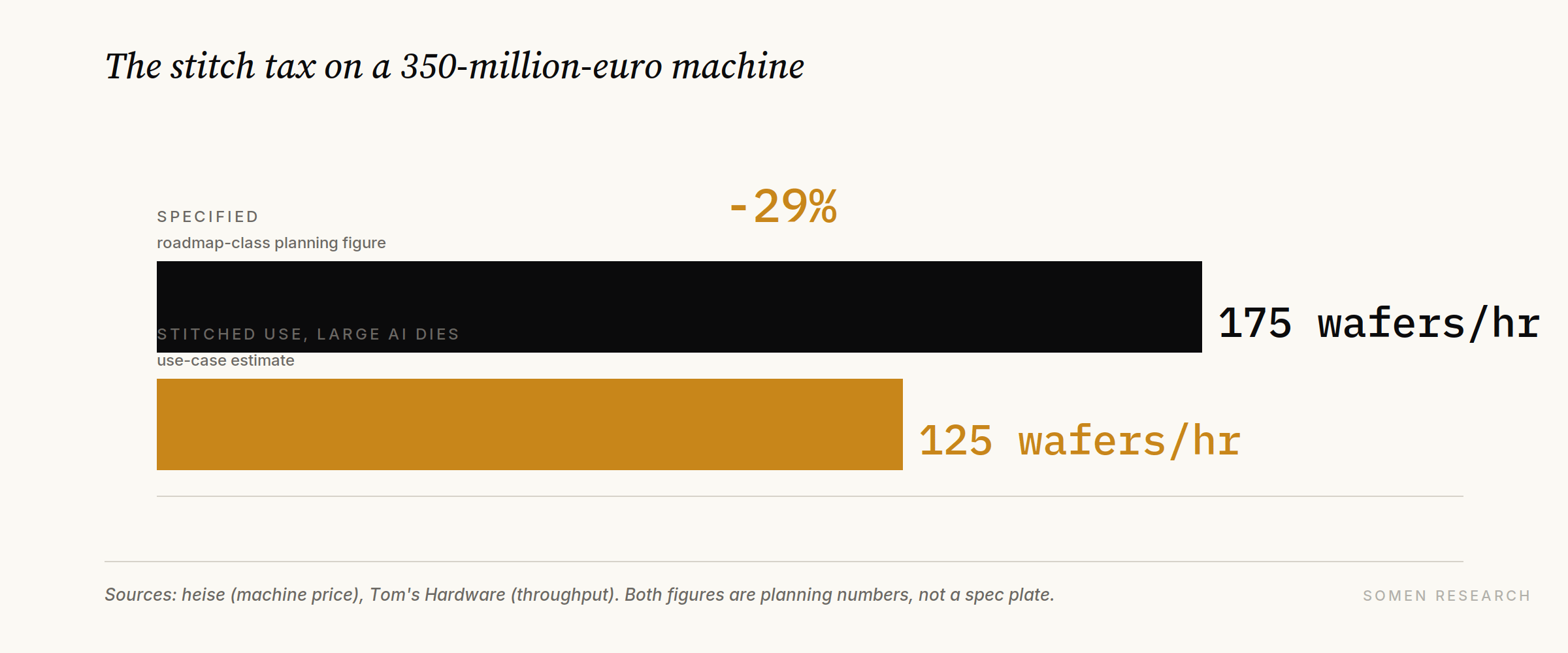
The most advanced chip printer on the market costs at least 350 million euros and is rated for 175 wafers an hour. On the giant dies at the center of the AI buildout, it delivers 125. Nothing is broken. The stencil is too small.
The machine is ASML’s High NA scanner. Extreme ultraviolet (EUV) lithography prints circuits with light dozens of times finer than visible light, and High NA (numerical aperture, in essence how fine the optics focus) sharpens the picture enough for the coming generations of chips. The sharpening has a price. The optics shrink the stencil’s pattern eight-fold in one direction and four-fold in the other, so a single exposure covers half the area it used to: 26 by 16.5 millimeters instead of 26 by 33. The stencil itself does not shrink, which is exactly why the fix turns out to be a longer one. A chip bigger than the field must be stitched from two exposures that have to line up, and stitching costs throughput: the specified 175 wafers an hour becomes 125 in stitched use, with every seam a defect risk.
On September 7 and 8, around a photomask conference in Monterey, three joint statements landed: the initiative itself from ASML and TSMC, with parallel announcements from ASML and Intel Foundry and from ASML and Samsung. The industry would move the photomask itself, the physical template every chip is printed from, off the 6-inch square that has been the standard since the 1990s and onto a 6-by-12-inch rectangle (the announcements say “12-inch”; the object is ruler-shaped, not square). A pilot line by 2031. Production-ready lithography systems by 2033. The mask restores the full exposure field, and large dies print in one pass.
The releases describe broad industry support. Two facts sit underneath. The commercial suppliers who must build the larger glass, coat it, write it, and inspect it are not named in any of the three statements; the attendee list is undisclosed. And the one large supplier speaking on the record about the advanced merchant mask market, America’s Photronics, told investors in August it is waiting for that market to become, in its own words, “effectively economically viable” before committing full capital.
That gap is this piece. An announced clock, and a public record with no vendor signature on it.
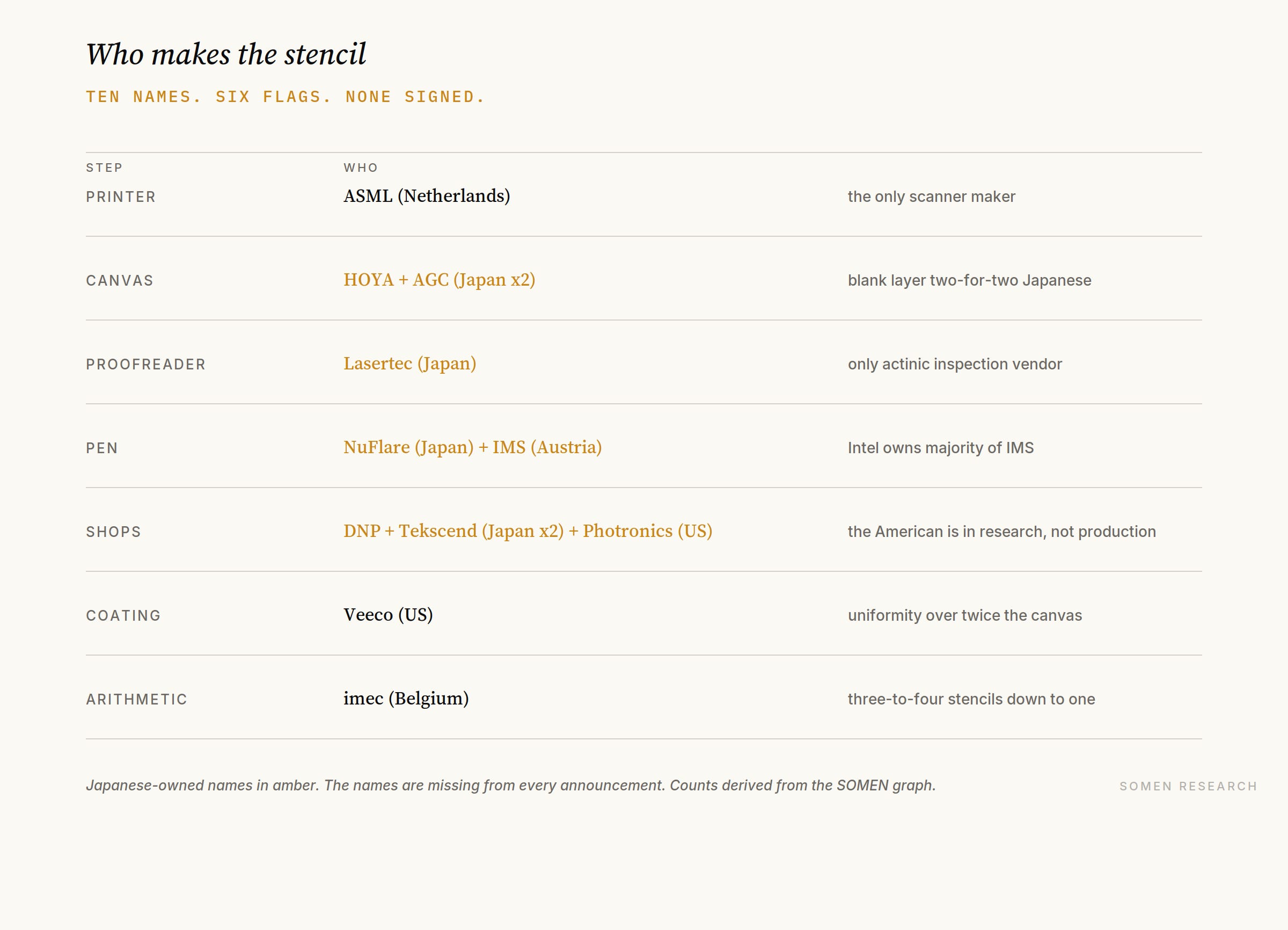
Our graph tracks ten named suppliers across the six tool classes a High NA mask passes through: scanner, blanks, inspection, writers, mask shops, and deposition. Six of the ten are Japanese. The blank layer, the coated glass plate every mask starts as, is two-for-two Japanese. The largest American supplier is in the research layer and out of the production round. No Chinese company appears anywhere in the record; the attendee list is undisclosed, so that is a safe inference rather than a documented exclusion, and the reason runs deeper than invitations.
The short version:
A 350-million-euro machine runs at 71 percent of its rating because the stencil is too small. The industry response is a bigger stencil, on a 2031/2033 clock.
The tool classes that would build it are six-tenths Japanese, blank layer two-for-two, and the largest US merchant shop says the advanced market is not yet worth entering.
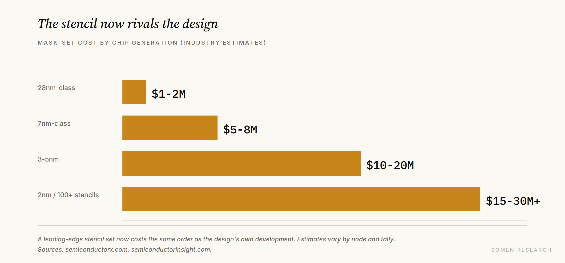
At the leading edge the stencil set now rivals the design it prints in cost.
China’s workaround for banned EUV printers multiplies its consumption of the one layer it cannot localize, bought from suppliers who control its export license.
The route, for the skimmer: the supply stack first (who makes this thing), then the calendar (when), then the arithmetic (what it costs), then who captures the value, and last the China side of the same layer. Each section stands alone. The watchlist at the end is the scoreboard, and the table beneath it grades every load-bearing figure in the piece.
The stack
The cast first, because the jargon is about to arrive. ASML is the only maker of the printers. TSMC, Samsung, and Intel manufacture most of the world’s advanced chips and buy those printers. Every printer needs a stencil, the photomask, and the stencil has its own supply chain: six kinds of shop stand between a blank plate of glass and the finished template. Think of a stencil the way a printer thinks of it: a canvas, a pen, a proofreader, and a wrapper, each made by one or two companies.
The canvas. Every EUV mask begins as a blank, a plate of glass engineered not to expand with heat, polished flat and coated with dozens of alternating layers that reflect the printing light. Two suppliers in the world make qualifying EUV blanks. HOYA’s own investor review claims an “exceptionally high market share” in EUV blanks, with a development roadmap already committed through High NA and the generation after. AGC describes itself as “the world’s only manufacturer of EUVL mask blanks that can handle every aspect from glass materials to coating”, and it expanded its Koriyama plant by roughly 30 percent in 2025 under a Japanese government supply-chain subsidy. High NA blanks need flatter glass and tighter defect criteria than the current generation, and they sell for more, not less.
The pen. The pattern is written onto the blank by beams of electrons, and the writer layer is a two-house market, one of each flag. NuFlare of Japan shipped its newest multi-beam writer, the MBM-4000, in the third quarter of 2025, aimed at an upcoming chip generation and at High NA mask production. IMS Nanofabrication of Austria, majority-owned by Intel, supplies the other merchant multi-beam line. The format change redoubles the writers’ economics: a 12-inch mask carries twice the write area of a 6-inch one, so every format-era mask is more writer-hours, and more writer demand, than the mask it replaces. The writer houses are the quiet beneficiaries of the standard the customers announced.
The proofreader. Inspection is a one-company gate. Lasertec is the only vendor whose machines check a finished mask using the same light that will print it, the method called actinic inspection, and its A300 inspects today’s High NA stencils, the 6-inch anamorphic kind, through the protective film. Every EUV mask in production qualifies on a Lasertec. The 12-inch class is a separate entry on its published roadmap, “large mask support”, alongside the generation beyond High NA.
The shops. The mask itself is made in a shop: captive (the big chipmakers’ own in-house operations) or merchant (for hire). The three big chipmakers make their advanced masks in-house. The merchant layer is led by two Japanese houses. Dai Nippon Printing finished qualifying its mask process for High NA in December 2024 and has shipped evaluation masks since. It is bringing its second and third multi-beam writers into operation and targets mass production of masks for the 2-nanometer chip generation in fiscal 2027. And Tekscend, the former Toppan Photomask, runs a five-year joint High NA mask research program with IBM, signed in 2024, and is separately expanding capacity in Singapore.
Then there is the shop that is not in the announcements. Photronics, the largest American merchant mask maker, producing down to 7 nanometers in Boise and advancing toward 4, spent August explaining why it is not rushing. It supplies EUV research masks through partnerships “while the full turnkey EUV merchant market develops”, in the words of its earnings call, and will enter when it makes sense “to catch the wave”. A full internal EUV program would cost about 300 million dollars, its investor-relations chief said the next day, which is why the company wants the return before the dive. The read is structural, not a knock: the advanced mask market is dominated by the captives, so the merchant tier rationally waits.
But note who the captives buy from. The blank maker’s own investor review lists semiconductor foundries among its customers, and the writer and inspection houses sell across the industry, captive shops included. The shops can sit out; the tool base cannot. The subscription that gates a 2031 pilot line is the tool vendors’, and theirs are the names missing from every announcement.
The coating, and the arithmetic. Back at the start of the biography, the coating itself is a physics problem. Veeco, the US deposition-tool vendor, modeled what it takes to coat a 6-by-12 blank uniformly: recovering coating uniformity across a 104-by-264-millimeter active area, roughly twice today’s canvas, is where the format change becomes process engineering before it becomes capital spending.
And underwriting every adoption date is imec, the Leuven research institute that received one of the first High NA systems in March and qualifies it through late 2026. Its arithmetic is the only hard number beneath the calendar: on the layers that decide how dense a chip can be, today’s EUV needs three to four separate stencils where High NA needs one.
The stack in one line: two Japanese canvas makers, two pen houses flying different flags, one proofreader, two Japanese merchant shops plus an American waiting one out, one coating physicist, and one research institute holding the arithmetic. Six of the ten names are Japanese, and every one of them is a name missing from the announcements.
The clock
The timeline has three dates, and they read as sequencing more than deadlines: each step assumes the one before it. Samsung says it will run High NA in mass production of DRAM, the main memory type, by 2028, the first time anyone uses the technology in memory at scale. TSMC intends High NA in high-volume logic manufacturing from 2030, and it is the only company that put a public date on the 12-inch format itself: pilot line 2031, production readiness 2033. Intel does not need a date; it already runs High NA on select production layers, and its statement is a ledger: more than one million wafers, the silicon discs chips are cut from, processed in under two years, which its partner ASML’s figures make more than the rest of the industry combined, up from roughly 30,000 at the start of 2025.
The schedule is deliberately staged, a technical read of the initiative notes: the industry adopts the new optics first, between 2028 and 2030, on current 6-inch masks with stitching, and the new mask infrastructure second. Changing both at once is the failure mode the staging avoids. ASML’s chief executive said the same thing in one sentence at the launch: adoption rises “progressively along the device scaling roadmap, first using current 6-inch masks and then further supported by 12-inch masks”. The clock is not ceremony. Every year the largest dies spend on its far side is a year they carry the stitching tax.
SK hynix is the honest hedge in the middle. It installed the industry’s first High NA system inside a mass-production fab, at M16 in Icheon, aimed at DRAM process simplification. It also placed an 11.95-trillion-won order, about 8.4 billion dollars over two years, for standard EUV tools that roughly double the existing fleet. On the 12-inch initiative itself, it told reporters it is evaluating membership. One machine for the next era, a fleet for this one, and no signature yet on the format. Micron, the third memory maker, names no optics class at all for its next node, a fork we track separately.
The arithmetic
What does the template cost? A single EUV stencil runs roughly half a million to one million dollars, an ultra-flat plate carrying a near-flawless reflective coating. A full set for a 3-to-5-nanometer chip design runs 10 to 20 million dollars across 70 to 100 stencils, with some tallies reaching 30 to 50 million, and the 2-nanometer class carries 100 or more. These are industry estimates and they vary; the direction does not. At the newest geometries, the stencil set and the design’s own development cost are the same order of magnitude. The stencil now rivals the design it prints, which pushes new chip designs toward the high-volume products that can spread that cost out.
On the other side of the ledger is what the bigger stencil buys. Stitching takes the machine from a specified 175 wafers an hour to 125 in stitched use, a loss of roughly 29 percent; restored, that is about a 40 percent gain, a figure ASML’s chief technology officer put publicly at the Monterey announcements, by one relay’s account. Both numbers are planning figures, a roadmap target and a use-case estimate, not a spec plate. And one question the figure deserves: whether printing the full field returns all the speed depends on whether the machine’s limit is its light or its moving parts, a detail ASML has not published. The 40 percent is ASML’s own net accounting, not a law of optics. For a buyer whose accelerators press the size limit, the format change buys back roughly a third of a 350-million-euro machine. The arithmetic cannot lobby you.
The demand side is explicit. Standard EUV prints chips up to about 800 square millimeters, and companies like NVIDIA and Google design right to that limit; High NA’s smaller field currently caps die size below it, which is why ASML says it will work with its largest customers to adapt the tools to the big data-center chips they design. The 12-inch mask is the mechanism that re-opens single-pass printing for exactly those dies, and the productivity case runs on three axes at once. The same scan exposes twice the field, spreading the scanner’s depreciation over more good dies per hour. Stitching disappears, along with its seam-yield risk. And the mask swaps a stitched design forces go away.
And before a single 12-inch stencil ships, every coating, inspection, and measurement step in the chain re-qualifies over twice the active area.
Who pays, who profits
Intel holds three seats at this table. It is the largest High NA user, with the wafer count to prove it. It majority-owns one of the two writer houses, IMS. And it has championed the 12-inch format for more than three years, working the standards and the supplier ecosystem long before Monterey made the timeline public. The company that ran the most wafers also owns a piece of the writer demand those wafers create.
The re-tool spreads across everyone who uses EUV, not just the High NA buyers. The format would spread to today’s standard EUV machines too, in the reading of a mask-industry executive roundtable, which also concluded that every tool involved in making stencils would need to be redesigned or replaced to varying degrees: writers, etchers, inspection, measurement, cleaning, pellicles, handling. Mask shops face outfitting for both formats at once, and companies not ready for large-format risk losing access to the newest scanner generations. One humility note from the same roundtable: the finest assist features may need about 15-nanometer resolution on the stencil, and the limit is the light-sensitive coating, not the pen.
Worth holding the initiative’s own language against its structure. The announcement says High NA adopters and other major suppliers “have expressed their interest” in joining. Interest is not a contract, a capex line, or a delivery date, and 2031 is five years out for tools that take years to develop and qualify. The bull case writes itself: three customers with captive shops carry the pilot, and the tool vendors follow their largest accounts as they always have. The open question is timing, not eventual participation, and the gap between “expressed interest” and a signed tool contract is where this supply chain’s schedule risk actually lives.
Japan’s position in this layer rests on three levers. Market position, the map above. Subsidy, the METI supply-chain program behind AGC’s expansion, the one on record. And the export license, which is the next section.
The wall
On the far side of the initiative sits the country that cannot buy the newest printers at all. China’s route to near-frontier chips runs on the previous generation of machines, pushed as far as a trick called multi-patterning will go: printing the same layer several times with shifted stencils to fake detail finer than the machine can draw in one pass. That route multiplies China’s consumption of the one input it cannot make at home.
The mechanics: the finest layers of a 7-nanometer-class chip built this way need about four printing passes where the EUV path needs one, and a 5-nanometer-class push would need six to eight. Every pass is another stencil, another alignment step, another opportunity for defects, and the printing stage alone is roughly half of a chip’s total manufacturing time.
The ceiling, from teardowns of Huawei’s Kirin 9030: SMIC’s latest process reaches about 113 million transistors per square millimeter, roughly the density of TSMC’s N6, by pushing its finest wiring to 32.5-nanometer pitch, below the conventional DUV cliff, using self-aligned quadruple patterning, which prints a coarse pattern and lets deposited spacer films define the fine lines. EUV-class density without EUV, at yield-challenged, cost-penalized economics. Manufacturing persistence instead of superior lithography.
The layer beneath: Chinese brokerage assessments put high-end blank production at home at effectively zero, with the more demanding phase-shift variety of blanks for the previous-generation lithography “almost zero” and domestic output concentrated in display panels and legacy lines. The state’s answer, by the same assessments, is an acquisition of a Korean blank maker’s business, a supplier certified at SK hynix and more than a generation ahead of anything domestic. And the domestic scanner champion’s output, about five of the older immersion-type tools in 2026, is capped by delays in components imported from Japan.
The measurement burden compounds with the stencil count. Every added pass needs its own alignment and dimension checks, so measurement demand scales with pass count, and measurement is the thinnest layer of China’s domestic tool set, roughly a quarter made at home against better than 40 percent for etching equipment. The supporting cast around the printer, writers and inspection and coating equipment and blanks, is concentrated in the same handful of countries across the board; even China’s component suppliers depend on foreign sub-suppliers for optics, lasers, and stages.
The rules already reach the stencil. Japan’s 2023 export controls added 23 categories of chipmaking equipment, and separately listed EUV pellicles, the protective film over the stencil, as their own controlled item, components and technology included. The United States added its own layer in December 2024, written to cover tools and measurement equipment regardless of which chip generation they serve. The stencil layer sits inside two live export-control perimeters. This is not a hypothesis about what a future restriction might cover; the coverage exists in force.
This multiplies China’s demand for the exact stack it cannot make at home, blanks and writers and inspection and film, bought from the suppliers who control its export license. The software side of this separation is its own story, covered by us here; the hardware side is this one, and unlike software it compounds: every chip-generation push multiplies the stencil count again.
The watchlist
This is a structural read of a supply chain, not a trade call, and it is graded in public. The scorecard entry resolves by June 30, 2027. What would move it:
The clock slips. The 2031 pilot or 2033 readiness moves right, or Samsung’s 2028 memory commitment and TSMC’s dated pledge walk back.
The capex story collapses. ASML and TSMC confirm existing High NA tools can be retrofitted for the 12-inch format, shrinking the two-format re-tool burden.
The monopoly cracks. A second vendor ships stencil inspection that uses the printing light itself, at production grade.
The round stays empty. No named supplier contracts by the 2027 SPIE cycle, or the merchant tier is still unsubscribed going into 2027. This is the near-term test of the gap this piece leads with.
The wall develops a door. China joins a large-format standards effort, ships production EUV stencils, or the domestic blank-production line moves off zero.
Hedges on the record: scanner prices and throughput figures are the industry’s standard estimates, not published list prices. The 40 percent restore figure is a single relay of a public remark, and whether printing the full field returns the full rating depends on light-versus-motion limits ASML has not published. Stencil-set costs are analyst tallies and they vary. The China blank figures are brokerage assessments and the Kirin numbers are teardown-derived, both attributed as such. Samsung’s 2028 is a memory clock and TSMC’s 2030 is a logic clock, and the two are never the same sentence’s claim.
Counts in this piece derive from the graph at edit time: 124 companies, 13,967 edges, ten named mask-layer suppliers, six Japanese. The map is the record.
- The SOMEN Desk